Hardware Setup
CPU Installation
JP19, JP20, JP40, JP41, JP55
|
JP19 |
JP20 |
CPU-Type |
|
1-2 |
1-2 |
Intel P24D/P24T |
|
1-2 |
2-3 |
Intel i486, AMD 486, UMC U5S |
|
2-3 |
1-2 |
Cyrix M6/M7 |
|
2-3 |
2-3 |
reserved |
|
JP40 |
JP41 |
JP55 |
CPU type |
|
1-2, 3-4 |
1-2 |
Open |
Intel P24T/P24D/i486DX2/i486DX AMD Am486DX/DXs/DXL/DXL2 Cyrix Cx486 DX |
|
1-2, 3-4 |
1-2 |
Short |
Cyrix Cx486DX/DX2 (M7) |
|
1-2, 3-4 |
2-3 |
Open |
Intel i487SX |
|
2-3 |
Open |
Open |
Intel i486SX Cyrix Cx486S (M6) UMC U5S |
Note: JP55 is the Cyris CPU clock multiplier selection jumper for the older version of Cyrix CPU. For new version, this jumper can be left open.
CPU SMI/SMM Setting
JP 45-49, JP42, JP39, JP53, JP54
JP39/42:
2 4 6 8 10 12
o o o o o o
o o o o o o
1 3 5 7 9 11
For Intel 486 DX2/DX/SX, AMD DX2/DX
|
JP45-49 |
2-3 Short |
|
JP42 |
All Open |
|
JP39 |
All Open |
|
JP53 |
Open |
|
JP54 |
2-3 Short |
For Intel 486DX2/SX2/DX/SX SL enhanced CPU
|
JP45 |
1-2 Short |
|
JP46-49 |
2-3 Short |
|
JP42 |
All Open |
|
JP39 |
7-8 9-10 11-12 Short |
|
JP53 |
Short |
|
JP54 |
2-3 Short |
For Intel P24D/P24D
|
JP45-49 |
1-2 Short for P24D 2-3 Short for P24T |
|
JP42 |
All Open |
|
JP39 |
7-8 9-10 11-12 Short |
|
JP53 |
Short |
|
JP54 |
2-3 Short |
For Cyrix Cx486S/Cx486DX/Cx486DX2
|
JP45-49 |
2-3 Short |
|
JP42 |
All Open |
|
JP39 |
All Open |
|
JP53 |
Short |
|
JP54 |
2-3 Short |
For Intel 80486DX4
|
JP45-49 |
2-3 Short |
|
JP42 |
All Open |
|
JP39 |
7-8 9-10 11-12 Short |
|
JP53 |
Short |
|
JP54 |
1-2 Short |
CPU Clock Setting
JP36, JP37
|
JP37 |
JP36 |
CPU Clock |
|
Open |
Short |
50 Mhz |
|
Short |
Open |
40 Mhz |
|
Short |
Short |
33 Mhz |
|
Open |
Open |
25 Mhz |
JP44
This jumper is used to adjust the CPU Clock for the VESA Add-on cards compatiblity purpose.
1-2 Short: CPU clock delay
2-3 Short: CPU Clock in phase with SIS85C471 Chipset (default)
JP50 Clock Multiplier
|
JP50 |
Clock Multiplier |
|
Open |
3 |
|
1-2 |
2,5 |
|
2-3 |
2 |
Voltage Regulator Setting
P1, P2, P3
1-2 for 5V CPU
2-3 for CPU as below
P4
1 o o 2 Close + 3,3 V
3 o o 4 Close + 3,45V
5 o o 6 Close + 3,6 V
7 o o 8 Close + 4,0 V
Note: Only one position can be closed in a time!!
Cache SRAM Installation
Cache Jumper Setting
JP25-28: TAG RAM setting
JP21-24: DATA SRAM setting
|
Cache
|
Tag SRAM Size |
JP28 |
JP27 |
JP26 |
JP25 |
Cachable Range WB |
Cachable Range WT |
|
32k |
2k*8 |
2-3 |
2-3 |
2-3 |
2-3 |
4MB |
8MB |
|
64k |
4k*8 |
1-2 |
2-3 |
2-3 |
2-3 |
8MB |
16MB |
|
128k |
8k*8 |
1-2 |
1-2 |
2-3 |
2-3 |
16MB |
32MB |
|
256k |
16k*8 |
1-2 |
1-2 |
1-2 |
2-3 |
32MB |
64MB |
|
512k |
32k*8 |
1-2 |
1-2 |
1-2 |
1-2 |
64MB |
128MB |
|
1MB |
64k*8 |
1-2 |
1-2 |
1-2 |
1-2 |
128MB |
128MB |
.
|
Cache
|
Data SRAM Type |
Q'ty |
Banks |
JP21 |
JP22 |
JP23 |
JP24 |
|
32k |
8k*8 |
4 pcs. |
1 |
1-2 |
1-2 |
1-2 |
1-2 |
|
64k |
8k*8 |
8 pcs. |
2 |
2-3 |
1-2 |
2-3 |
2-3 |
|
128k |
32k*8 |
4 pcs. |
1 |
1-2 |
2-3 |
1-2 |
1-2 |
|
256k |
32k*8 |
8 pcs. |
2 |
2-3 |
2-3 |
2-3 |
2-3 |
|
521k |
128K+8 |
4 pcs. |
1 |
1-2 |
2-3 |
1-2 |
1-2 |
|
1MB |
128k*8 |
8 pcs. |
2 |
2-3 |
2-3 |
2-3 |
2-3 |
Onboard Peripherials
Serial Port (J7/J8) Setting
JP2, JP3 COM1
|
JP2 |
JP3 |
COM1 Address |
|
1-2 |
1-2 |
3F8 (Default) |
|
1-2 |
2-3 |
2F8 |
|
2-3 |
1-2 |
3E8 |
|
2-3 |
2-3 |
disabled |
JP4, JP5 COM2
|
JP4 |
JP5 |
COM2 Address |
|
1-2 |
1-2 |
2F8 (Default) |
|
1-2 |
2-3 |
3F8 |
|
2-3 |
1-2 |
2E8 |
|
2-3 |
2-3 |
disabled |
JP29 IRQ Selection
1 o | o 2
3 o | o 4
1-2 - COM1 IRQ3
3-4 - COM2 IRQ4
1-3 - COM1 IRQ4 (Default)
2-4 - COM2 IRQ 3 (Default)
Parallel Printer Port LPT1 (J9) Setting
JP2, JP3 COM1
|
JP8 |
JP9 |
LPT1 Address |
|
1-2 |
1-2 |
278 |
|
1-2 |
2-3 |
378 (Default) |
|
2-3 |
1-2 |
3BC |
|
2-3 |
2-3 |
disabled |
JP2, JP3 COM2
|
JP4 |
JP5 |
COM2 Address |
|
1-2 |
1-2 |
2F8 (Default) |
|
1-2 |
2-3 |
3F8 |
|
2-3 |
1-2 |
2E8 |
|
2-3 |
2-3 |
disabled |
JP30 IRQ Selection
1-2 - LPT1 IRQ5
2-3 - LPT1 IRQ 7 (Default)
Floppy Disk Drive Port (J4) Setting
JP6 1-2 FDD enable (Default)
JP6 2-3 FDD disable
JP11 1-2: 370 to 377 address range
JP11 2-3: 3F0 to 3F7 address range
JP17, JP18 FDD (2,88MB) Media ID Selection
1 o | o 1-2 Normal
2 o | o 2-3 FDD Media ID Input
3 o | o JP17: Media ID bit 1
JP18: Media ID bit 0
ISA IDE Port (J10) Setting
JP7 1-2 HDD enable (Default)
JP7 2-3 HDD disable
JP12 1-2 secondary (Default)
JP12 2-3 primary
JP32 1-2 IRQ 15 (Default)
JP32 2-3 IRQ 14
VL-BUS IDE Port (J6) Setting
JP38 1-2 enable (Default)
JP38 2-3 disable
Game Port (J8) Setting
JP10 1-2 enable (Default)
JP10 2-3 disable
VL-Bus ID Setting
JP51 Open VESA Clock <= 33 Mhz
JP51 Short VESA Clock > 33 Mhz
JP52 Open VESA high speed 0 wait
JP52 Short VESA high speed 1 wait
Note: The VESA clock is equal to the cpu-clock.
System Front Panel Connection
|
Connector |
Function |
Pin |
Assignment |
Activity |
|
J12 |
HDD LED |
1 2 3 4 |
+5V DC HDD active HDD active +5V DC |
On: Accessing Off: No active |
|
J13 |
Reset Switch |
1 2 |
Reset Input Ground |
Open: Normal Close: Reset |
|
J14 |
Turbo Switch |
1 2 |
Turbo Input Ground |
Open: Turbo Close: De-Turbo |
|
J15 (Note1) |
Turbo LED |
1 2 |
LED Anode LED Cathode |
On: Turbo Off: De-Turbo or green |
|
J16 |
Speaker |
1 2 3 4 |
DataOutput No connection Ground +5V DC |
. |
|
J18 |
Key Lock and Power LED |
1 2 3 4 5 |
LED Power No connection Ground Keyboard Inhibit Ground |
On: Power On Off: Power Off On: Lock Off: Un-Lock |
|
J19 (Note2) |
Power Saving Switch |
1 2 |
Active Inut Ground |
Open: Normal Close: Suspend |
Note1: When the system enter green mode, the turbo LED will be turn off to indicate this status.
Note2: The power saving switch uses a suggested break off type switch. The switch has no function when the green function is set to disable in the BIOS setup program.
CMOS and Battery Setting(JP1, J11)
JP1 1-2 normal operation (Anmerkung: handschriftlicher Eintrag !Open!)
JP1 2-3 Clear CMOS
Caution: Before shorting JP1 in 2-3 position to clear CMOS, first power off the mainboard and schould be kept 1-2 in normal operation.
J11 1-4 external battery
J11 2-3 Short: on board battery
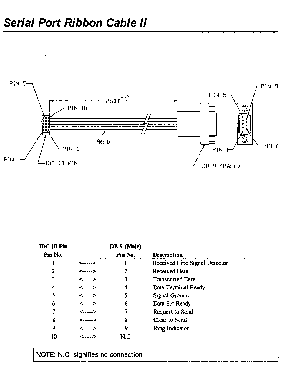
Cable Specification
Die Kabel für die COM-Ports scheinen nicht dem Standard zu entsprechen, jedenfalls kann ich nur die mit dem Rechner gekauften auf diesem Board verwenden.
Hier die gescannten Manualpages:
25pol. Serialkabel | 9pol. Serialkabel | Printerport
Mainboard Layout
ch471b.gif (40k)
BIOS-Millenium-Bug: use c't Y2k-Patch (18k)
Für weitere Fragen und Anregungen Email an mich
Danksagung:
Mein Dank geht an Andreas Koschel, Vobis-Mitarbeiter in Rudolstadt. Er hat mir freundlicherweise das Handbuch zu diesem Board überlassen.
Leider ist es heute noch nicht normal, zu Komplettsystemen die vollständige Dokumentation der Hardware mitzuliefern, so daß ein Aufrüsten durch den interessierten Bastler -wenn überhaupt- nur nach dem Try-and-Error-Prinzip funktioniert.